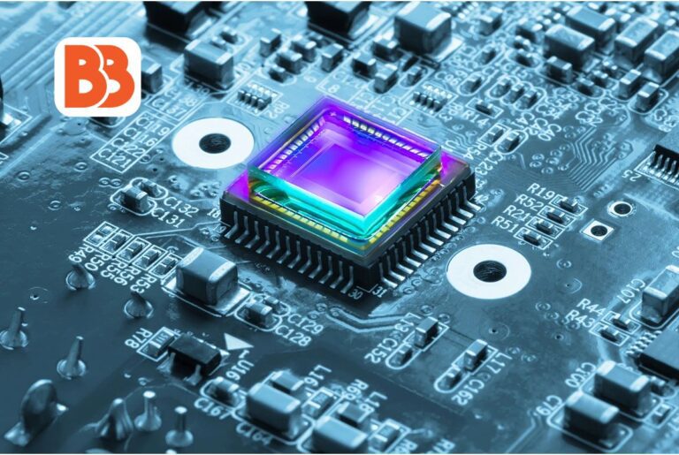
Chiplet technology is a new paradigm in semiconductor design and manufacturing aimed at overcoming the limitations of conventional monolithic chips. A chiplet is a small, modularized, special integrated circuit (IC) that can be combined to form larger and more complex system-on-chip (SoC) and multi-chip modules (MCM). Chiplets have several advantages over monolithic chips, such as high performance, low power consumption, high flexibility, reduced time to market, and low cost. In addition, the chiplet enables the integration of various functions and technologies into one package, such as processor, memory, I/O, fabric, analog, RF, sensor, photonics, etc. Let’s delve into this article to learn about “All about Chiplet Technology advanced PCB design”.
What is Chiplet Technology?
A chiplet is a compact integrated circuit (IC) with different functions. The purpose of the chiplet is to seamlessly integrate a single package with other chiplets on the interposer. The basic concept of Chiplet Technology is to break down the system-on-chip and make it a functional component. Chips with complex functions can be broken down into chiplets, each representing individual elements. Such as computational processors, graphics units, AI accelerators, I/O functions, and various other chip functions. A system consisting of a chiplet is similar to SoC on a module. In the future, chiplet components sourced from various providers can be mixed and matched interoperably. The placement of a chiplet can be likened to a versatile “Lego-like” assembly, offering more advantages than traditional system-on-chip designs.
Chipplet Architecture
The basic concept of a chiplet architecture is to decompose large and complex chips into smaller, simpler chiplets that each execute a specific function or domain. Chiplets are interconnected via substrates and interposers, such as wire bonding, flip chips, and micropumps. This interconnection enables high-speed, low-latency data transfer, communication between chiplets, and power and heat management. Chiplets can be manufactured individually using different process nodes, technologies and foundries and combined to form a complete system. You can read more about EVO 5.0: Unveiling the Next Generation Of Power and Innovation. It allows you to reuse existing IP blocks, optimize the functionality of each chiplet, and customize the system according to application requirements.
Advantages of Chiplet
Compared to monolithic chip technology, chiplet technology has the following advantages:
Scalability
Chiplets can be easily scaled up or scaled down by adding or removing a chiplet without affecting other parts of the system. It enables us to build heterogeneous and highly adaptable systems that meet various applications and market demands.
Performance
The Chiplet leverages each function’s best technology and process nodes to achieve higher performance than monolithic chips, avoiding single-chip performance bottlenecks and tradeoffs. Also, since the chiplets are close to each other and have a dedicated interconnection, data movement and latency in the system can be reduced.
Power
The chiplet operates at low voltage and frequency, the die size is small, and the parasitic is low, thus reducing the system’s power consumption and heat generation. In addition, the chiplet can be turned on and off individually or adjusted dynamically according to the workload, enabling fine-grained power management.
Cost
Chiplets reduce the complexity and risk of design, increase yield and reliability, and reuse existing IP and infrastructure, thus reducing system costs. In addition, chiplets can be designed and manufactured in parallel, making it easy to update and replace, reducing the time to market and development costs of the system.
Innovation
Chiplets can promote innovation in the semiconductor industry by integrating various new technologies such as AI, quantum, neuromorphic and optical computing into a single system. Chiplet also promotes cooperation and competition among various players in the industry. Including chip designers, IP providers, foundry, and system integrators, to realize a vibrant and dynamic ecosystem.
Example of a Chiplet
Here are some notable examples of Chipplet Technology’s potential being realized today.
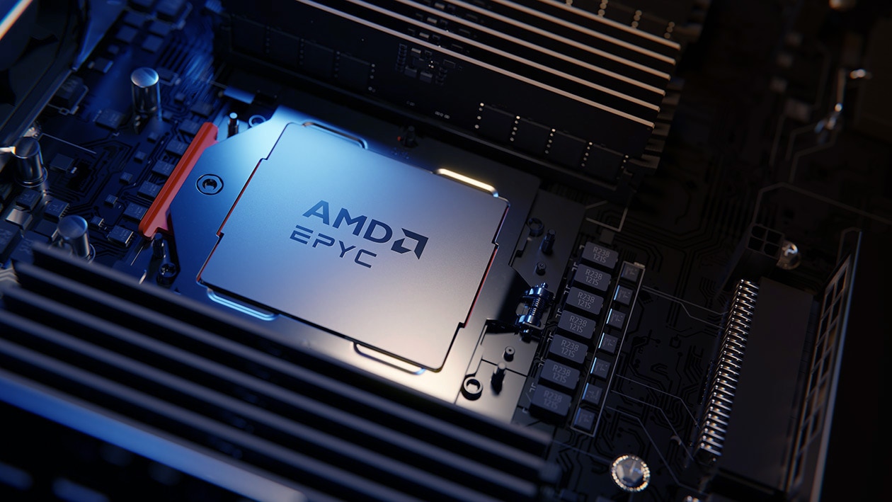
AMD Ryzen and EPYC processors
AMD’s Ryzen processor and EPYC processor line approach to adopt chiplets demonstrates significant improvements in performance and efficiency that can be achieved with a chiplet-based architecture. Introduced in the Zen 2 and later processor generations, AMD’s chiplet architecture utilizes multiple small chips (chiplets) connected via high-speed Infinity Fabric interconnections. This design allows AMD to scale performance and number of cores efficiently while maintaining cost efficiency and flexibility.

Intel EMIB
Intel’s Embedded Multi-die Interconnect Bridge (EMIB) is an innovative approach to packaging different semiconductor chips (chiplets) into one package to enable fast communication between chiplets. With this technology, heterogeneous chips such as CPU, GPU, and memory can be integrated into a single package to optimize performance and power efficiency.Notable applications of EMIB technology include Intel’s Stratix 10 FPGA and Agilex FPGA. Which support a wide range of applications from data centers to network infrastructure and embedded systems. Using EMIB, Intel offers a customized, high-performance computing solution that meets specific customer needs.
![[Eng Sub] Intel EMIB](https://i.ytimg.com/vi/hSQ_HAG2uoY/maxresdefault.jpg)
![[Eng Sub] Intel EMIB](https://i.ytimg.com/vi/hSQ_HAG2uoY/maxresdefault.jpg)
Versal ACAP
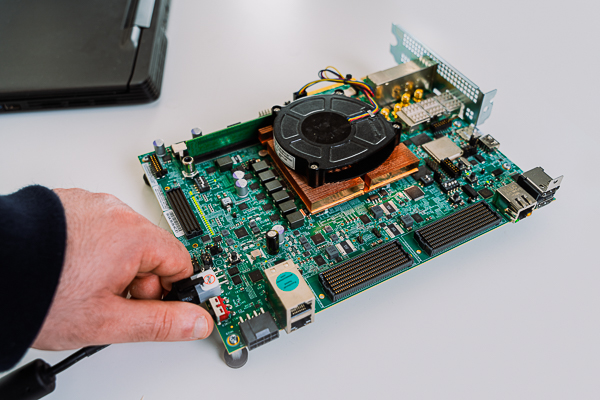
The Adaptive Compute Acceleration Platform (Versal ACAP) series provides powerful and flexible capabilities in the heterogeneous computer devices category, combining scalar processing engines, adaptive hardware, and intelligent engines with state-of-the-art memory and interface technologies.Versal ACAP series versatility and performance demonstrate the advantages of a chiplet-based design. These highly adaptable products meet various application needs, from network and cloud acceleration to embedded computing and AI inference.

Chiplet Challenges
Chiplet technology also has the following challenges and limitations:
Interconnectivity
Chiplets require high bandwidth, low latency, and low power interconnection for interactive and external communication. However, current interconnection technologies such as wire bonding, flip-chips, and micro-bumps may need help with the growing demand for chiplet systems, especially high-performance applications. Therefore, to maximize the potential of chiplet technology, it is necessary to develop and adopt new interconnect technologies. Such as silicon penetrating electrodes (TSV), silicon interposers, and chip-to-chip optical links.
Thermal Management
The chiplet generates heat during operation and affects performance, reliability and life. Therefore, it needs to be properly cooled and heat-controlled, but the it is implemented in high density. And the thermal characteristics and requirements are different, resulting in difficulties. In addition, thermal resistance and hot spots occur on the substrates and interposers that connect the chiplets, which can worsen heat problems. Therefore, it is necessary to consider and implement new thermal management technologies such as micro-fluid, thermoelectric. And phase change cooling to ensure optimal operation of the chiplet system.
Standardization
Common standards and protocols must be followed to ensure compatibility and interoperability between chiplets and systems. However, the current chiplet standards and protocols still need to be mature and complete. As their preferences and specifications vary depending on the chiplet provider and user. Therefore, the industry must cooperate and converge on universal standards and protocols for chiplets. Such as the Universal Chiplet Interface (UCIe), an open and royalty-free standard for chiplet communication and integration.
How does a chiplet change SoC design?
Chiplets revolutionize SoC design by realizing new levels of heterogeneity and modularity. The chiplet enables designers to utilize the advantages of various technologies and areas, such as logic, memory, analog, RF, photonics, etc., to realize high-performance, power-efficient electronics. By realizing a new paradigm of design automation, selecting, assembling, and optimizing chiplets. You can create highly customizable SoCs that meet specific design objectives and constraints.
As a result, the design workflow is becoming highly repetitive. And the traditional design center approach needs to be more varied, making it very time-consuming and efficient. Designers need agility and cross-sectoral collaboration to meet technology and market demands. It includes better concepts, designs and simulation tools that reduce insight time, eliminate unnecessary prototype spins, and eliminate knowledge silos.It is where Keysight’s Modern Design Center appears.
Conclusion
Chiplet technology provides new semiconductor design and manufacturing methods to overcome the limitations of conventional monolithic chips. And is a promising and destructive trend in the semiconductor industry. It enable scalable, high-performance, low-power, low-cost innovative systems to meet various applications and markets’ diverse and evolving needs. However, Chiplet technology brings several challenges and opportunities to the industry, including interconnectivity, thermal management, and standardization. To maximize the potential of chiplet technology, we need to solve and utilize these challenges.
Frequently Asked Questions
What is a Chiplet?
This is a small, self-contained integrated circuit block that performs certain functions. The chip designer combines multiple chiplets of different applications into a single chip package.
Why is a chiplet important for future processors?
Chiplets are important for the future of processors because they provide new semiconductor designs and manufacturing methods. That can overcome the limitations of conventional monolithic chips. Chiplets enable scalable, high-performance, low-power, and low-cost.
How is the chiplet interconnected and packaged?
Chiplets are interconnected and packaged in various ways, such as wire bonding, flip chips, micropumps, silicon-penetrating via (TSV), silicon interposers, and optical links between chips. This interconnection enables high-speed, low-latency data transfer and communication between chips and power and heat management.
